- 您现在的位置:买卖IC网 > Sheet目录3873 > PIC16F627-04/P (Microchip Technology)IC MCU FLASH 1KX14 COMP 18DIP
2003 Microchip Technology Inc.
Preliminary
DS40300C-page 59
PIC16F62X
10.0 VOLTAGE REFERENCE
MODULE
The Voltage Reference is a 16-tap resistor ladder
network that provides a selectable voltage reference.
The resistor ladder is segmented to provide two ranges
of V
REF values and has a power-down function to
conserve power when the reference is not being used.
The VRCON register controls the operation of the
reference as shown in Figure 10-1. The block diagram
is given in Figure 10-1.
10.1
Configuring the Voltage Reference
The Voltage Reference can output 16 distinct voltage
levels for each range.
The equations used to calculate the output of the
Voltage Reference are as follows:
if V
RR = 1: VREF = (VR<3:0>/24) x VDD
if V
RR = 0: VREF = (VDD x 1/4) + (VR<3:0>/32) x
V
DD
The setting time of the Voltage Reference must be
considered when changing the V
REF output
(Table 17-2). Example 10-1 shows an example of how
to configure the Voltage Reference for an output
voltage of 1.25V with V
DD = 5.0V.
REGISTER 10-1:
VRCON REGISTER (ADDRESS: 9Fh)
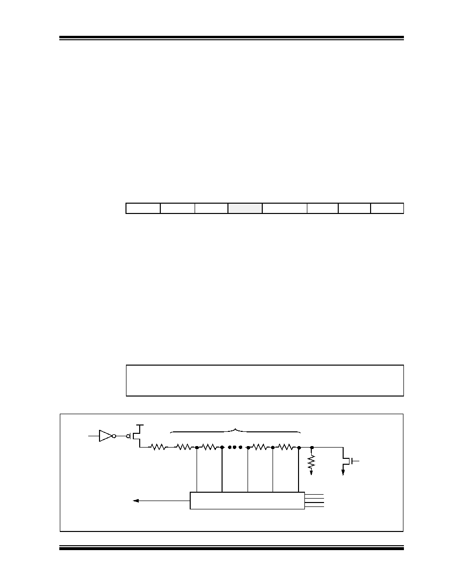
FIGURE 10-1:
VOLTAGE REFERENCE BLOCK DIAGRAM
R/W-0
U-0
R/W-0
VREN
VROE
VRR
—VR3
VR2
VR1
VR0
bit 7
bit 0
bit 7
V
REN: VREF Enable
1
= VREF circuit powered on
0
= VREF circuit powered down, no IDD drain
bit 6
V
ROE: VREF Output Enable
1
= VREF is output on RA2 pin
0
= V
REF is disconnected from RA2 pin
bit 5
V
RR: VREF Range selection
1
= Low Range
0
= High Range
bit 4
Unimplemented: Read as '0'
bit 3-0
V
R<3:0>: VREF value selection 0
≤ VR [3:0] ≤ 15
When V
RR = 1: VREF = (VR<3:0>/ 24) * VDD
When V
RR = 0: VREF = 1/4 * VDD + (VR<3:0>/ 32) * VDD
Legend:
R = Readable bit
W = Writable bit
U = Unimplemented bit, read as ‘0’
-n = Value at POR
’1’ = Bit is set
’0’ = Bit is cleared
x = Bit is unknown
Note
1: R is defined in Table 17-2.
Vrr
8R
Vr3
Vr0
(From VRCON<3:0>)
16-1 Analog Mux
8R
R
V
REN
Vref
16 Stages
V
DD
V
SS
V
SS
发布紧急采购,3分钟左右您将得到回复。
相关PDF资料
PIC18F45J10-I/ML
IC PIC MCU FLASH 16KX16 44QFN
PIC18F24K22-I/ML
IC PIC MCU 16KB FLASH 28QFN
PIC16CR76-I/SS
IC PIC MCU 8KX14 28SSOP
PIC16F887-I/P
IC PIC MCU FLASH 8KX14 40DIP
PIC16CR76-I/SP
IC PIC MCU 8KX14 28DIP
PIC16CR76-I/SO
IC PIC MCU 8KX14 28SOIC
PIC16CR76-I/ML
IC PIC MCU 8KX14 28QFN
PIC16CR74T-I/ML
IC PIC MCU 4KX14 44QFN
相关代理商/技术参数
PIC16F627-04/P
制造商:Microchip Technology Inc 功能描述:IC 8BIT FLASH MCU 16F627 DIP18
PIC16F627-04/SO
功能描述:8位微控制器 -MCU 1.75KB 224 RAM 16I/O 4MHz SOIC18 RoHS:否 制造商:Silicon Labs 核心:8051 处理器系列:C8051F39x 数据总线宽度:8 bit 最大时钟频率:50 MHz 程序存储器大小:16 KB 数据 RAM 大小:1 KB 片上 ADC:Yes 工作电源电压:1.8 V to 3.6 V 工作温度范围:- 40 C to + 105 C 封装 / 箱体:QFN-20 安装风格:SMD/SMT
PIC16F627-04/SO
制造商:Microchip Technology Inc 功能描述:8BIT FLASH MCU SMD 16F627 SOIC18
PIC16F627-04/SO
制造商:Microchip Technology Inc 功能描述:Microcontroller IC Number of I/Os:16
PIC16F627-04/SS
功能描述:8位微控制器 -MCU 1.75KB 224 RAM 16I/O 4MHz SSOP20 RoHS:否 制造商:Silicon Labs 核心:8051 处理器系列:C8051F39x 数据总线宽度:8 bit 最大时钟频率:50 MHz 程序存储器大小:16 KB 数据 RAM 大小:1 KB 片上 ADC:Yes 工作电源电压:1.8 V to 3.6 V 工作温度范围:- 40 C to + 105 C 封装 / 箱体:QFN-20 安装风格:SMD/SMT
PIC16F627-04E/P
功能描述:8位微控制器 -MCU 1.75KB 224 RAM 16I/O RoHS:否 制造商:Silicon Labs 核心:8051 处理器系列:C8051F39x 数据总线宽度:8 bit 最大时钟频率:50 MHz 程序存储器大小:16 KB 数据 RAM 大小:1 KB 片上 ADC:Yes 工作电源电压:1.8 V to 3.6 V 工作温度范围:- 40 C to + 105 C 封装 / 箱体:QFN-20 安装风格:SMD/SMT
PIC16F627-04E/SO
功能描述:8位微控制器 -MCU 1.75KB 224 RAM 16I/O 4MHz Ext Temp SOIC18 RoHS:否 制造商:Silicon Labs 核心:8051 处理器系列:C8051F39x 数据总线宽度:8 bit 最大时钟频率:50 MHz 程序存储器大小:16 KB 数据 RAM 大小:1 KB 片上 ADC:Yes 工作电源电压:1.8 V to 3.6 V 工作温度范围:- 40 C to + 105 C 封装 / 箱体:QFN-20 安装风格:SMD/SMT
PIC16F627-04E/SS
功能描述:8位微控制器 -MCU 1.75KB 224 RAM 16I/O 4MHz Ext Temp SSOP20 RoHS:否 制造商:Silicon Labs 核心:8051 处理器系列:C8051F39x 数据总线宽度:8 bit 最大时钟频率:50 MHz 程序存储器大小:16 KB 数据 RAM 大小:1 KB 片上 ADC:Yes 工作电源电压:1.8 V to 3.6 V 工作温度范围:- 40 C to + 105 C 封装 / 箱体:QFN-20 安装风格:SMD/SMT